Knowledgebase CCD - Reliable with premium quality
Sensors based on charge-coupled device (CCD) technology have driven the development of digital machine vision. Light-sensitive regions (photosites) in each pixel of the CCD chip convert incoming photons into electrical charge. Compared to CMOS technology, CCD sensors generally have a larger photosensitive area. This simplifies the illumination requirements in your application.
Simplicity is the strength of CCDs
The collected charge is transported in bucket brigades to the analog-to-digital converter (ADC). The most commonly used CCD sensors have a single ADC, which has little effect on the signal-to-noise ratio. CCD technology is still preferred for high performance images.
CCD based SVCam models from SVS-Vistek
SVS-Vistek offers a wide range of CCD cameras - with resolutions from VGA to 47 megapixels. Choose the camera that best suits your needs or contact us with your specific requirements.
Cameras from SVS-Vistek with CCD technologie (53)
The history of CCD
Originally, CCD elements (Charge-Coupled Devices) were used exclusively for the transport of electrical charge. As early as the 1970s, the photoelectric properties of the semiconductor material were put to practical use. This enabled the transport of charge generated by light in the CCD.
CCD even won the Nobel Prize
In 2009, the inventors of CCD technology received the Nobel Prize in Physics. The two laureates, George E. Smith and Willard S. Boyle, had been working on the generation and transport of electric charge at Bell Laboratories since 1965. Their work led to the application for a patent for this technology.
Sony mass production in Japan
Mass production of CCD chips proved more difficult than expected and was only carried out on a small scale in the USA. At Sony, Kazuo Iwama led a team of engineers toward the goal of commercial mass production of CCD sensors. Sony paved the way for the future. A CCD sensor still graces its tombstone today.

The operation of CCD
The bucket brigade principle
The analogy of buckets collecting raindrops is often used to explain how a CCD collects and transports electrons. Photons release electrons from the semiconductor material and store them as a negative charge in a "bucket" called a potential well. By applying a positive voltage to a gate, the negative electrons are captured in the potential well. By moving the voltage across the wells in a sequence, the charge is moved from one well to the next. Much like water is moved in a bucket brigade.
CCD sensor readout
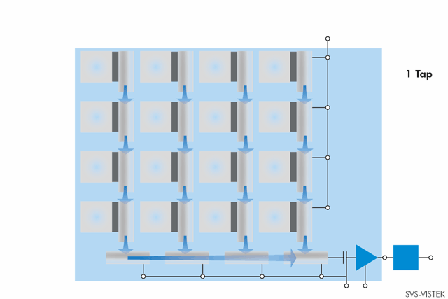
At the end of the exposure time, the charge is transported from the light-sensitive surface to the vertical shift registers. These are organized as columns and transport the charge downward like a bucket brigade. Row by row, the charge is transported to the horizontal shift register of the CCD sensor, which operates at a much higher speed. At the end of the horizontal shift register is an amplifier and an analog-to-digital (A/D) converter.
The architecture described above is called "interline frame transfer".
CCD data rates
Due to the inherent design of CCD sensors, their readout rate is slower compared to CMOS sensors. By applying additional readout structures, commonly referred to as "taps", the readout rate can be doubled (dual-tap sensors), quadrupled (quad-tap sensor), or made even faster by adding additional taps. (For more ways to increase CCD speed, see the "PIV Mode" section). Contact us to learn more about how advanced CCD timing schemes can be used in your specific application.
Performance-limiting effects
Amplifiers and analog-to-digital converters (ADC) usually have the greatest impact on performance. Their operation is not strictly linear. Most CCD sensors have only a single set of these elements and therefore have little impact on the image. Sensors with multiple readout structures (taps) then have multiple amplifiers and ADC converters. Due to the non-linearity, additional signal processing may be required to adjust the output levels (tap balancing).
Blooming
Blooming can be compared to an overflowing bucket. When too many electrons accumulate on the photo side, the charge begins to overflow onto the neighboring pixels. On the captured image, blooming shows up as a large circular spot resembling a blooming flower in the center of the oversaturated area. This can be circumvented with an anti-blooming drain that limits the maximum charge in a pixel. This is similar to a drain hole just below the rim of a bucket.
Smearing
At high light intensities, you may see vertical lines in the image. These are called smearing. The smearing occurs directly in the vertical shift registers. After reading out the image, the shift registers through which the CCD pixel information is passed to the amplifier may themselves be light sensitive.
In photo cameras, this is avoided by a mechanical shutter that protects the chip during readout. In image processing cameras, this is attempted to be avoided by the design of the chip.
Feel free to contact us, we will be happy to advise you on the various options for reducing performance-reducing effects.