Knowledgebase CMOS - Flexible and fast sensor technology
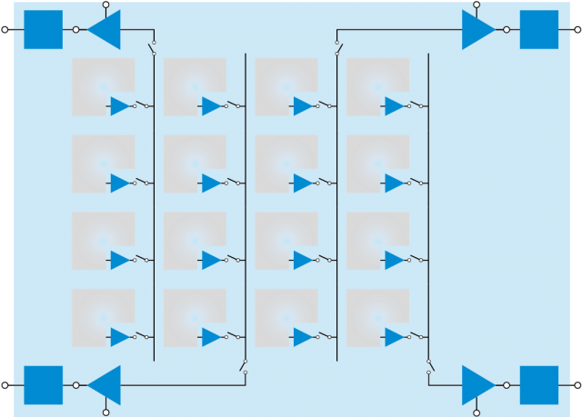
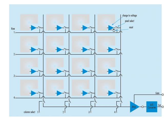
In a typical CMOS sensor each pixel has its own amplifier and there are multiple A/D converters. Each picture element can be read out individually, the reason these sensors are referred to as “Active Pixel Sensors”.
Complex technology permits ease of use
Simultaneous readout means that pixels can be randomly addressed and accessed, making several areas-of-interest, AOIs, (or regions-of-interest, ROIs) possible. For early adopters this, combined with the advantage low power dissipation, outweighed the poorer noise performance. Current designs have, however, greatly overcome the noise issue.
The CMOS sensor technology adopted by SVS-VISTEK all have performance equivalent to CCDs. Put them to the test and convince yourself.
SVCam from SVS-VISTEK with CMOS technology
Cameras with CMOS technology from SVS-VISTEK provide a full suite of resolution, ranging from 1 to 25 megapixel. Choose one that matches your needs, or contact us with your specific requirements.
SVCam Serien mit CMOS-Sensoren (236)The history of CMOS technology
In the mid-90s, Eric Fossum at NASA Jet Propulsion Laboratory was successful in creating an Active Pixel Sensor. He made use of CMOS technology for reading out the photodiode. CMOS technology dates back to the 60s. CMOS (Complementary Metal Oxide Semiconductor), is based on a transistor design capable of handling both positive and negative charge. CPU and memory chips found in devices we use daily, are commonly based on CMOS technology.
The underlying technology of CMOS
The incident light causes he junction of a diode oriented in the reverse direction to be discharged. At the end of the exposure time, the remaining voltage of the diode is read out.
CMOS only denotes the architecture of the read-out mechanism. CMOS uses p and n channel MOSFET transistors in pairs. This design results in low power dissipation. Resistors are not required for CMOS technology. Current therefor only flows momentarily when the diode is read out.
Read more about the specifics of Sony Exmor Pregius -technologie and their equivalents from other manufacturers of CMOS sensors.
CMOS technology drawbacks
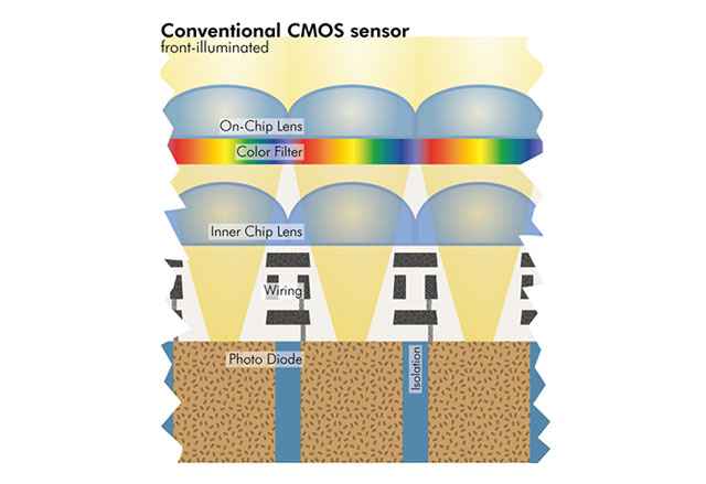
CMOS sensors have a reputation of poor signal-to-noise ratio. This has two distinct sources: The high number of transistors and A/D-converters and the low fill factor (the ratio between the light sensitive area and the total pixel area). The relatively low fill factor of many CMOS sensors is due to the high integration density on the chip.
Deficiencies can be overcome
The advances in the manufacturing of CMOS sensors have profited from the general development in the semiconductor industry. Higher integration density becomes possible as transistors shrink in size, while performance increases. Limited fill factor can be overcome with micro-lenses. A method also commonly applied to CCD sensors.
Process related
The fundamental architecture of a sensor chip limits its ability to collect light. The conducting layers are deposited on top of the light sensitive structure of the semiconductor material. The advantage of collecting light on the rear surface of the chip is well known. Engineers attempting to implement this on a broad scale were faced with numerous challenges. Light in the visible spectrum only penetrates the substrate to a depth of 5 to 10 micrometers. Backside illuminated sensors require the semiconductor wafer material to be greatly reduced in thickness. To achieve the desired performance, the substrate must not only be thinned, but also have an even surface.
CMOS advantages
The costs for manufacturing CMOS sensors are lower. In addition, CMOS sensors allow for more compact designs.
Smearing and blooming are both a thing of the past with CMOS technology.
Partial images, fields or areas-of-interest (AOIs) can be read out simultaneously.
The low power dissipation simplifies temperature management. Performance limitation due to over-heating is ruled out.